Velleman K8000 - DAC High Power Amplifier - The circuit
The image below shows my complete schematic for this project. You can click it to increase the size or you can download it as a PDF.
A first look at the schematics may give a complicated impression but in fact the circuit is very easy to understand. The circuit has some major parts: the rectifier, the FET voltage generator, the voltage stabilizer, the voltage controller, the reverser circuit and the control for the reverser circuit.
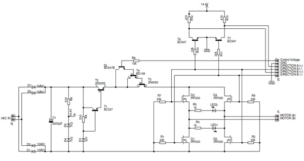
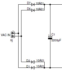
The rectifier turns the AC voltage from the transformed into a DC voltage. It is built with a bridge of 4 power diodes. I used power diodes that can withstand currents of up to 10 A.
After the rectifier there is a large capacitor to flatten the DC voltages. I chose a value of 2200 µF but it will need to be increased if you plan to control high currents with the circuit.
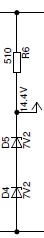
The FET Voltage generator gives a stable 14.4 V voltage to control the FET polarity reverser. This voltage is obtained by two zenerdiodes with a value of 7.2 V. They are placed in series so this adds up to 14.4 V.
The output current of the voltage generator is limited: I measured currents of up to 30 mA.
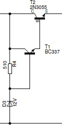
The following part is the voltage stabilizer: it will create a stable output voltage. The stabilizer is very basic: a zenerdiode is used to generate the reference voltage.
The zener D3 will create a stable 12 V output voltage. This voltage then is applied to transistors T1 and T2. Each time the voltage passes a B-E junction of a transistor the voltage decreases with 0.7 V. This means the output voltage is 12 V - 0.7 V - 0.7 V = 10.6 V
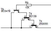
The voltage stabilizer made us just a stable 10.6 VDC voltage which doesn't depend on the current. This voltage now needs to be controllable from 0 ... 10 V. This is done by the voltage controller. It is built with 3 transistors: T3,T4 and T5.
The control voltage from the K8000 is applied to the base of transistor T5. There is a 10k resistor to restrict the current. Under normal circumstances this resistor almost has no effect on the output voltage of the circuit as the current through it is very low.
Each transistor will now pass its emitter voltage to the base of the next transistor. Each one of these transistors is more powerful. The 2N3055 is a power transistor that can handle currents of up to 15 A!
Just as with the voltage stabilizer each B-E junction will cause a voltage drop. The total voltage drop between control voltage and output will be 3 * 0.7 V = 2.1 V. This means the maximal output voltage of the circuit is about 8.5 - 9 V.
Warning: The 2N3055 is a power transistor that can handle currents of up to 15 A. It will get hot and should be cooled with a heat sink. You should be aware a lot of power is dissipated in this component. This value can rise above 100 Watts! (this can happen when you set a low output voltage while there is a large output current).
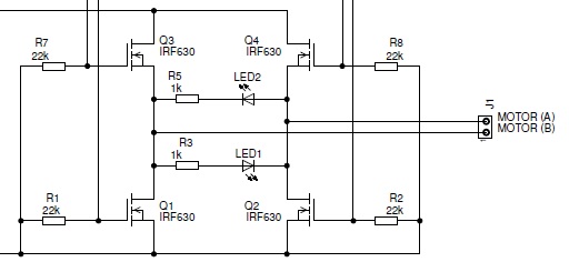
The reverser circuit can toggle the output polarity(+/- or -/+). When you use the circuit to control a motor the direction of the rotation will change. To be able to do this I built a bridge with 4 N-Channel FETs. At any time only 2 FETs are conducting at the same time: Q1/Q4 or Q2/Q3.
Activating all FETs at the same time is a very bad idea: it would simply create a short circuit. Obviously this should be avoided at all times. I have therefore added a protection circuit (see 'reverser control circuit')
A N-channel FET starts conducting by applying a positive voltage to the gate. This opens a channel between the Drain and Gate connections. To have the channel fully conducting the voltage at the gate must be a few volts higher than the voltage at the source.
This isn't a problem for the FETs Q1 & Q2 as their source connection is directly connected with the GND. Another story for the FETs Q3 & Q4: when one of them conducts its source voltage equals the output voltage of the circuit, which can be any value between 0 and 9 V.
The trick here is to apply a voltage that is a few volts higher than the output voltage. It's for this reason I added a FET voltage generator to the circuit: it gives 14.4 V and therefore it is always some volts higher than the maximal output voltage of the circuit.
I have chosen power FETs (IRF630N). They have a Rds (on) resistance of only 0.2 Ohm. This means they almost don't dissipate any power.
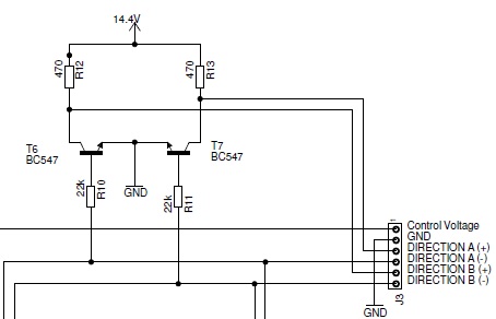
In the previous topic you could already read the 4 FETs may never be activated at the same time. I designed an extra circuit to avoid this ever happens. The circuit has 2 transistors and 4 resistors: T6 and T7, R10 to R11.
Normally none of these two transistors is conducting since there is no voltage at its base. In this case the voltage at their collectors equals the FET control voltage: 14.4 VDC.
To activate the motor DIRECTION A you need to connect the pins "DIRECTION A+" and "DIRECTION A-" all together. Doing so will cause the 14.4 VDC from the collector of transistor T7 is brought to the gates of the FETs 2 & 3. They start conducting.
This same voltage is also brought to the base of transistor T6 which causes it to start conducting. This will cause the voltage at its collector drops to almost 0 V. In this situation there is no voltage at the connection "DIRECTION B+" so connecting it with "DIRECTION B-" simply doesn't have any effect.
Short summary: there are two transistors: one for each pair of FETs. The activation of one transistor prevents the other one from being activated. This: only the direction that is activated first will be used.
Warning: you should always use direct connections to connect the DIRECTION- and DIRECTION+ together. If there is a resistance between them - and therefore a voltage drop - there will be a lower voltage at the gates of the FETs. This causes the two upper FETs to have a higher power dissipation: THEY HEAT UP.
![]()
![]()
Copyright ©1998-2022 Vanderhaegen Bart - last modified: August 24, 2013
