ELECTRONICS - [RS-232 Interface] - [page 2/4]
The circuit for the interface is not hard to understand. It only has a few ICs. The image below shows the schematic diagram. You can click the image to enlarge it. Alternatively you can download the schematic as a PDF.
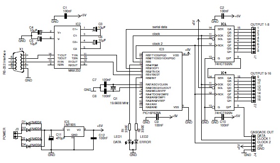
The circuit accepts any input voltage (AC or DC). You should use at least 8 or 9 V input voltage. Four diodes will rectify this voltage. The capacitor C1 will flatten it, while the LM7805 will convert it to a stable 5 VDC output signal. This voltage is used to power all digital IC's in the circuit. Be careful when you use this circuit to drive a lot of LEDs: the LM7805 might need some cooling. You will probably need to increase the value of capacitor C11 as well.
The interface itself is built around the microcontroller PIC 16F628A. This PIC is driven by a fast 19.6608 MHz crystal. I have chosen this crystal because its frequency is a perfect match for the data transmission speed between PIC and computer: 9600 baud.
The PIC outputs TTL-levels (0V/5V) while the serial port requires positive or negative voltages (+9V/-9V): a voltage level adjustment is required. This is the task of the MAX232 IC, which is placed between the serial port and the PIC. The surrounding capacitors are used for the internal charge pump (The MAX232 is powered by 5 V, but it needs to output higher voltages).
The circuit drivers two indication LEDs: DATA and ERROR. The DATA LED will invert each time a single byte is received. The ERROR LED will be activated in the case of a communication problem: when there are framing errors or when the checksum of the incoming data is incorrect.
I have used 8-bit shift registers to control the outputs. These registers will convert a serial stream of bits to parallel outputs. A shift register is easy to understand. The following image shows how a shift register works:
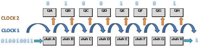
The shift register has a data input, which gets its data from the microcontroller. This data is passed bit by bit. Each time a new bit is placed, a clock pulse is generated. The bit will then enter the first stage of the shift register. The bit is now hold by the first stage (shift A). Every time a new clock pulse is given, an internal rotation/shift will occur. The bit will now shift from stage to stage each time a new clock pulse occurs: G shifts to H, F -> G, E -> F, D -> E, C -> D, B -> C, A -> B. The register A will get the value of the new incoming bit.
Notice the values of these stages won't appear at the outputs of the shift register (QA to QH) immediately. This won't happen until a second clock pulse is given (CLOCK 2). After this pulse the data from the internal registers is transferred to the output stages. The stages will hold this data (they are D-type flip-flops, triggered by the CLOCK2).
It is possible to cascade several shift registers: the output of the first shift register is then connected to the input of the following register. Both registers share their clock lines. My PIC hardware will allow to cascade up to 15 shift registers together. (I must admit I never tested this because I don't have that much shift registers).
This circuit shows only two shift registers, but you can additional shift registers to the connector CASCADE OUT. You can also choose to use only one shift register: it all depends on your requirements!
There is one important thing to consider: you can connect multiple shift registers which all share the same clock signals. The clock inputs of these registers have a certain capacitance. This capacitance is not big - just a few picofarats - and can be ignored when using a single shift register. Things change when using multiple shift registers: all those small capacitances will form a large equivalent capacitance. It then might be necessary to slow down the clock speed of the shifting process.
![]()
![]()
Copyright ©1998-2022 Vanderhaegen Bart - last modified: August 24, 2013
