ELECTRONICS - [solder station protection] - [page 3/5]
In the image below you can find the complete schematic for the soldering station protection.
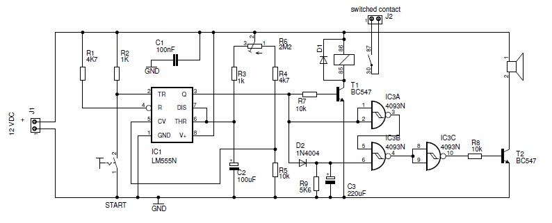
The circuit should be powered by a 12 VDC stabilized voltage. I have not added it to the schematics but it is easy enough to create this voltage with a single 7812 regulator. This is voltage regulator that will provide a stable output voltage.
The timer can be triggered by pressing the START button. This will connect the pin #2 of the 555 to the ground.
The other components around the 555 define its behavior. The potmeter R6 is used to regulate the duration of the timer. You can increase the maximum duration by replacing capacitor C2 with a higher value (220 µF, ...). I did this to increase the total time to 30 minutes.
The sound circuit will start sounding a buzzer when the timer elapsed. For this I have added 3 NAND gates, diode D2, resistor R9 and capacitor C3. They are connected to the output of the 555.
The basic idea is the capacitor C3 will charge when the output of the timer is active: it is charged through diode D2, which prevents the capacitor can affect the output of the 555. Even when the output of the 555 becomes low the voltage over the capacitor will still remain high for some time. It slowly discharges over the resistor R9.
This voltage will now be compared with the output voltage of the 555, using the NAND gates: If there is a voltage over capacitor C3 while the output of the 555 is low this is an indication the timer just stopped. This means the buzzer has to sound. The buzzer will sound only for a few seconds, until the capacitor C3 discharged. The discharge rate of the capacitor C3 is determined by its value and the value of the resistor R9. The higher one of these values is, the longer it takes to discharge.
I have added a truth table to make you better understand what is going on in the NAND gates. Even though Ucap is an analog voltage (it can have any values) I represented it as a digital value. Basically the output value of the 555 is inverted and then AND'ed with the capacitor state.
| U 555 | U cap | IC3A (out) | IC3B (out) | IC3C (out) |
| 0 | 0 | 1 | 1 | 0 |
| 0 | 1 | 1 | 0 | 1 |
| 1 | 0 | 0 | 1 | 0 |
| 1 | 1 | 0 | 1 | 0 |
The output of the IC3C drives the buzzer through transistor T2. This transistor provides the current needed to power the buzzer. The buzzer I used is a 12 VDC buzzer.
![]()
![]()
Copyright ©1998-2022 Vanderhaegen Bart - last modified: August 24, 2013
