ELECTRONICS - [I²C board] - [page 2/5]
Here you can find the complete schematic diagram for the I/O expansion board. You can click the image to enlarge it.
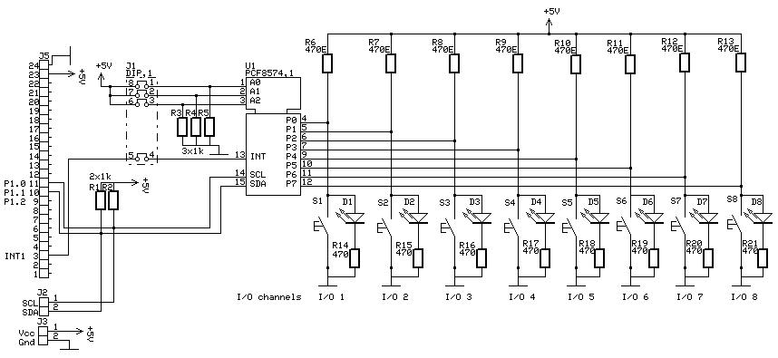
The circuit is built around a PCF8574 IC. This is an I2C port expander from Philips. This chip controls 8 I/O ports: you can either control LEDs or switches with it, depending on the requirements for your application. Note: I showed both of them on the schematic diagram.
Resistors R6 to R13 are pull-up resistors. They are keeping the I/O ports of the chip "high" during normal circumstances. Closing one of the switches S1 to S8 will make the respective port "low".
The address of the PCF8574 is selected by setting dip switch 1. There are 3 address lines so you can set 8 different addresses (0 - 7).
The SCL/SDA lines are for the communication with the I2C bus. They are connected to the two pull-up resistors R1 and R2.
You might notice all signals are split towards different connectors. The first 24-pin connector is to connect the board to a flat cable. As you could read earlier, this PCB was designed to be used with a 8051 test board. You don't have to use this connector: there are also two 2-P screw terminal connectors foreseen on the PCB: one for the supply voltage (5 VDC) and one for the SCL/SDA connections.
Attention:
The communication connector has only 2 pins: SCL and SDA. If you want to connect different systems you need to make sure the GND lines are all connected together. Otherwise the I2C communication will not work.
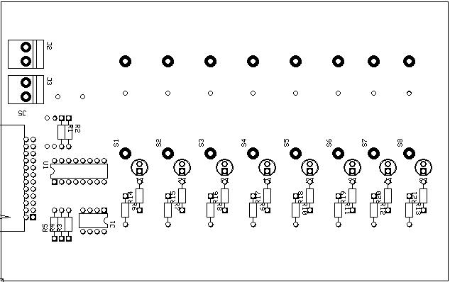
Component placing (Click picture to enlarge)
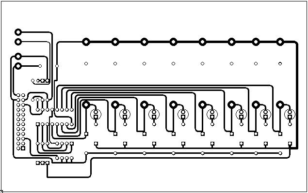
Solder side (Click picture to enlarge)
![]()
![]()
Copyright ©1998-2022 Vanderhaegen Bart - last modified: August 24, 2013
